1. Product Principles and Structural Characteristics of Alumina Ceramics
1.1 Crystallographic and Compositional Basis of α-Alumina
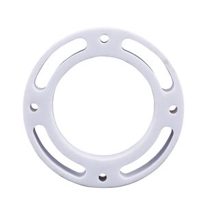
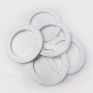
(Alumina Ceramic Substrates)
Alumina ceramic substratums, mainly made up of light weight aluminum oxide (Al ₂ O FIVE), act as the backbone of contemporary digital product packaging due to their phenomenal equilibrium of electrical insulation, thermal security, mechanical stamina, and manufacturability.
One of the most thermodynamically steady stage of alumina at heats is diamond, or α-Al Two O FIVE, which crystallizes in a hexagonal close-packed oxygen latticework with light weight aluminum ions occupying two-thirds of the octahedral interstitial sites.
This thick atomic arrangement conveys high hardness (Mohs 9), exceptional wear resistance, and strong chemical inertness, making α-alumina ideal for severe operating settings.
Industrial substratums usually contain 90– 99.8% Al Two O THREE, with minor additions of silica (SiO ₂), magnesia (MgO), or uncommon planet oxides used as sintering aids to advertise densification and control grain growth during high-temperature processing.
Greater pureness qualities (e.g., 99.5% and above) display premium electrical resistivity and thermal conductivity, while reduced purity variants (90– 96%) provide economical services for much less demanding applications.
1.2 Microstructure and Defect Design for Electronic Reliability
The efficiency of alumina substrates in digital systems is critically depending on microstructural uniformity and defect minimization.
A penalty, equiaxed grain framework– typically ranging from 1 to 10 micrometers– makes sure mechanical stability and decreases the likelihood of split proliferation under thermal or mechanical tension.
Porosity, especially interconnected or surface-connected pores, have to be reduced as it deteriorates both mechanical toughness and dielectric performance.
Advanced processing strategies such as tape casting, isostatic pushing, and controlled sintering in air or managed ambiences allow the manufacturing of substrates with near-theoretical thickness (> 99.5%) and surface roughness listed below 0.5 µm, essential for thin-film metallization and wire bonding.
Additionally, impurity partition at grain boundaries can lead to leakage currents or electrochemical movement under predisposition, necessitating rigorous control over raw material pureness and sintering problems to make certain long-lasting integrity in moist or high-voltage environments.
2. Production Processes and Substrate Manufacture Technologies
( Alumina Ceramic Substrates)
2.1 Tape Casting and Eco-friendly Body Handling
The production of alumina ceramic substratums begins with the prep work of an extremely distributed slurry containing submicron Al ₂ O five powder, natural binders, plasticizers, dispersants, and solvents.
This slurry is refined via tape spreading– a continual technique where the suspension is spread over a moving carrier movie making use of an accuracy physician blade to achieve consistent density, generally between 0.1 mm and 1.0 mm.
After solvent dissipation, the resulting “eco-friendly tape” is versatile and can be punched, drilled, or laser-cut to form by means of openings for vertical affiliations.
Numerous layers may be laminated to develop multilayer substratums for complex circuit combination, although the majority of commercial applications use single-layer setups because of cost and thermal expansion considerations.
The green tapes are after that thoroughly debound to eliminate natural additives through regulated thermal decay before final sintering.
2.2 Sintering and Metallization for Circuit Combination
Sintering is performed in air at temperatures between 1550 ° C and 1650 ° C, where solid-state diffusion drives pore removal and grain coarsening to achieve full densification.
The straight contraction during sintering– generally 15– 20%– have to be specifically forecasted and made up for in the design of environment-friendly tapes to make certain dimensional accuracy of the last substrate.
Adhering to sintering, metallization is put on create conductive traces, pads, and vias.
Two main techniques control: thick-film printing and thin-film deposition.
In thick-film innovation, pastes consisting of metal powders (e.g., tungsten, molybdenum, or silver-palladium alloys) are screen-printed onto the substratum and co-fired in a minimizing environment to form durable, high-adhesion conductors.
For high-density or high-frequency applications, thin-film procedures such as sputtering or dissipation are used to deposit bond layers (e.g., titanium or chromium) followed by copper or gold, allowing sub-micron patterning via photolithography.
Vias are full of conductive pastes and fired to establish electrical affiliations between layers in multilayer layouts.
3. Functional Features and Performance Metrics in Electronic Systems
3.1 Thermal and Electrical Habits Under Operational Anxiety
Alumina substrates are valued for their favorable mix of modest thermal conductivity (20– 35 W/m · K for 96– 99.8% Al ₂ O ₃), which makes it possible for efficient warm dissipation from power devices, and high volume resistivity (> 10 ¹⁴ Ω · centimeters), ensuring marginal leakage current.
Their dielectric continuous (εᵣ ≈ 9– 10 at 1 MHz) is secure over a vast temperature and frequency variety, making them appropriate for high-frequency circuits approximately several gigahertz, although lower-κ materials like light weight aluminum nitride are favored for mm-wave applications.
The coefficient of thermal expansion (CTE) of alumina (~ 6.8– 7.2 ppm/K) is reasonably well-matched to that of silicon (~ 3 ppm/K) and particular packaging alloys, decreasing thermo-mechanical tension throughout device operation and thermal biking.
However, the CTE mismatch with silicon remains a worry in flip-chip and direct die-attach configurations, frequently needing certified interposers or underfill materials to reduce exhaustion failure.
3.2 Mechanical Effectiveness and Ecological Longevity
Mechanically, alumina substratums show high flexural toughness (300– 400 MPa) and outstanding dimensional stability under tons, enabling their use in ruggedized electronics for aerospace, automobile, and commercial control systems.
They are immune to resonance, shock, and creep at elevated temperatures, maintaining structural stability up to 1500 ° C in inert ambiences.
In humid environments, high-purity alumina reveals minimal dampness absorption and superb resistance to ion migration, making certain long-term reliability in exterior and high-humidity applications.
Surface area firmness likewise secures against mechanical damages throughout handling and assembly, although treatment should be taken to prevent edge damaging due to intrinsic brittleness.
4. Industrial Applications and Technical Impact Throughout Sectors
4.1 Power Electronic Devices, RF Modules, and Automotive Solutions
Alumina ceramic substrates are common in power electronic modules, consisting of insulated gateway bipolar transistors (IGBTs), MOSFETs, and rectifiers, where they give electric seclusion while assisting in warm transfer to heat sinks.
In superhigh frequency (RF) and microwave circuits, they work as service provider platforms for hybrid incorporated circuits (HICs), surface acoustic wave (SAW) filters, and antenna feed networks as a result of their stable dielectric buildings and reduced loss tangent.
In the automobile industry, alumina substrates are made use of in engine control units (ECUs), sensing unit packages, and electrical vehicle (EV) power converters, where they withstand heats, thermal biking, and exposure to harsh liquids.
Their reliability under rough conditions makes them vital for safety-critical systems such as anti-lock stopping (ABDOMINAL MUSCLE) and progressed vehicle driver help systems (ADAS).
4.2 Clinical Instruments, Aerospace, and Emerging Micro-Electro-Mechanical Systems
Past consumer and commercial electronics, alumina substratums are used in implantable medical gadgets such as pacemakers and neurostimulators, where hermetic sealing and biocompatibility are extremely important.
In aerospace and defense, they are made use of in avionics, radar systems, and satellite communication components as a result of their radiation resistance and stability in vacuum settings.
Additionally, alumina is increasingly made use of as a structural and shielding platform in micro-electro-mechanical systems (MEMS), including pressure sensors, accelerometers, and microfluidic tools, where its chemical inertness and compatibility with thin-film processing are useful.
As digital systems remain to require higher power thickness, miniaturization, and reliability under extreme conditions, alumina ceramic substrates remain a cornerstone product, linking the void in between performance, price, and manufacturability in advanced electronic product packaging.
5. Vendor
Alumina Technology Co., Ltd focus on the research and development, production and sales of aluminum oxide powder, aluminum oxide products, aluminum oxide crucible, etc., serving the electronics, ceramics, chemical and other industries. Since its establishment in 2005, the company has been committed to providing customers with the best products and services. If you are looking for high quality kyocera alumina, please feel free to contact us. (nanotrun@yahoo.com)
Tags: Alumina Ceramic Substrates, Alumina Ceramics, alumina
All articles and pictures are from the Internet. If there are any copyright issues, please contact us in time to delete.
Inquiry us